Wafer Level Packaging Services for 3D IC, Flip Chip, WLCSP
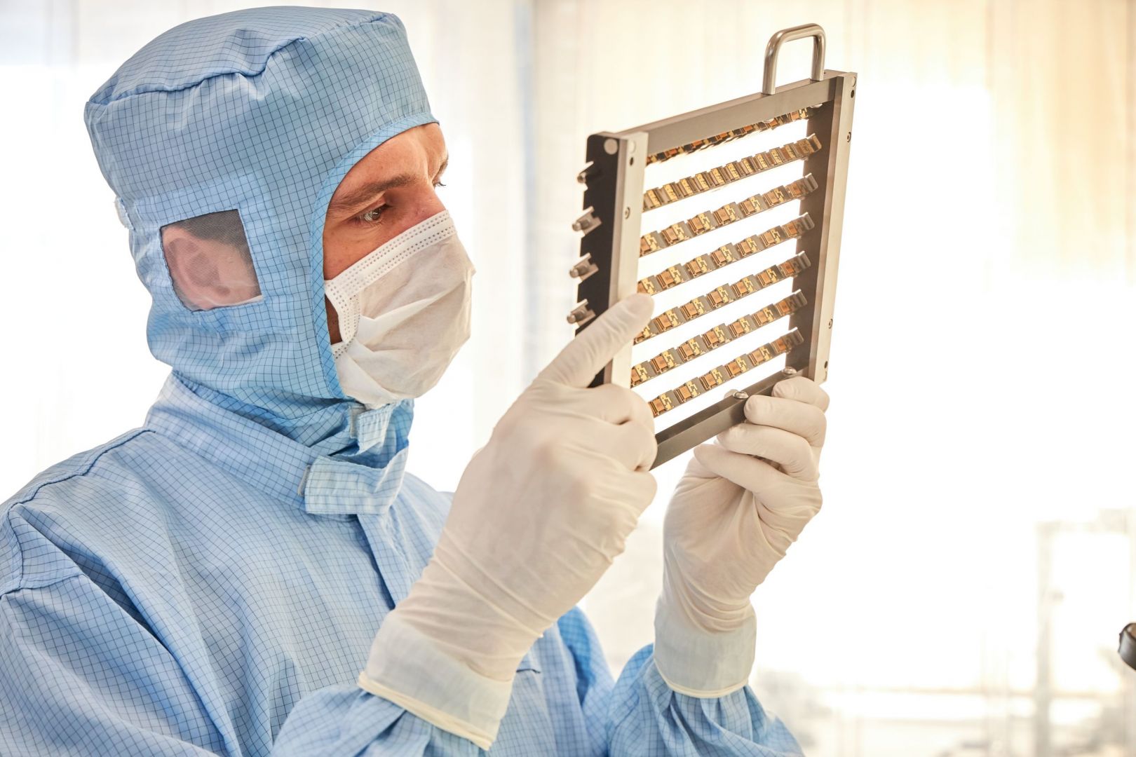
Being the pioneer of wafer level electroless plating technologies, PacTech has been offering WLP services to the semiconductor and electronics industry with over 25 years of experiences. We have been constantly expanding our WLP capabilities and developing cutting edge technologies in order to support packages in higher density and smaller size.
We provide various metallization finishes via different technologies including electro-plating, electroless plating, sputtering and evaporation. There are various solder bumping capabilities including solder printing, ball placement, electro-plated solder bump as well as Cu pillar which cater to specific layout design and assembly requirements.
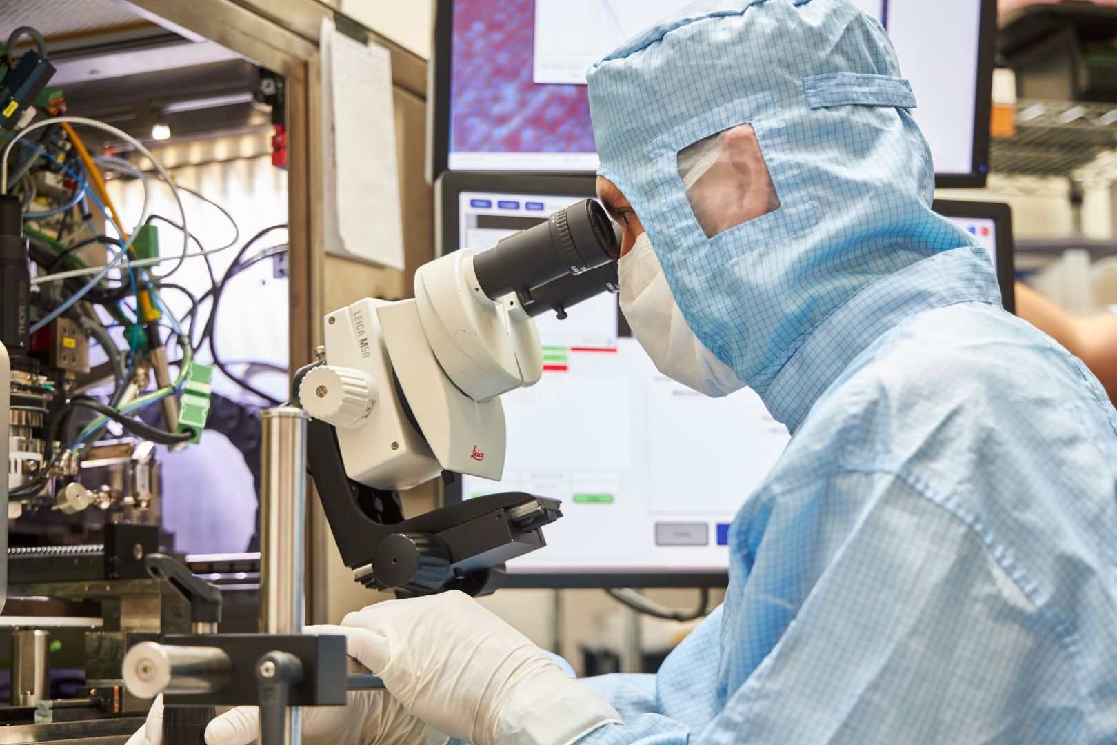
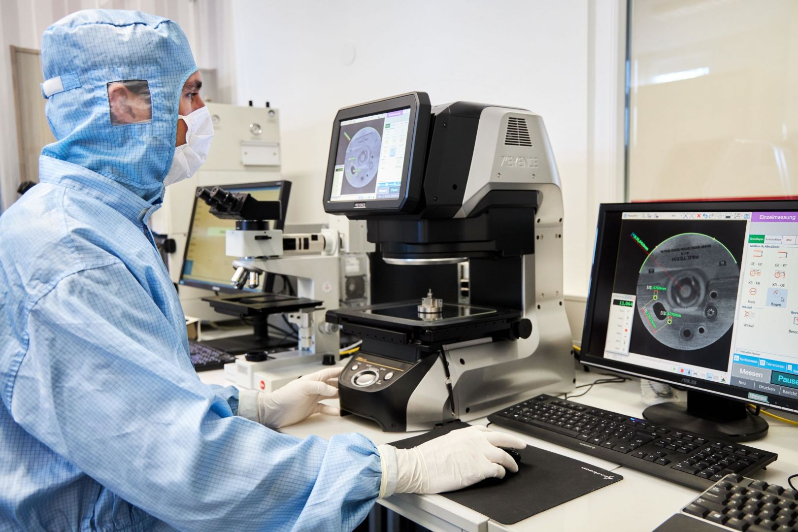
In addition, PacTech owns the latest metrology and analytical equipment to help in the development and production processes, including: X-ray, shear test, AOI, FIB, SEM, high speed ball pull, chemical analysis, etc.
We offer WLP services across the globe from all three PacTech sites in Europe, America and Asia, with professional WLP specialists to recommend the best performance and cost-effective solutions, supporting customized process development out of mainstream offers, and our flexible subcontracting model can be modified to suit different demand and loading strategies.
Our certified WLP service site in Europe fulfills the necessary security requirements according to international safety and security regulations for handling and processing sensitive and highly confidential customer products.
Our WLP services are being engaged in wide-range of industry applications, including automotive, aerospace, agriculture and farming, commercial, communication, industrial power, 5G and RF and many more. They are suitable for numerous assembly and packaging applications, such as: