ADVANCED PACKAGING EQUIPMENT

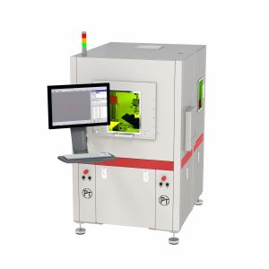
PacTech’s laser solder jetting technology is clean, precise, and flexible. Our unique ball handling mechanism supplies a separated single solder ball into the capillary where the laser beam’s thermal energy melts the solder ball, and the solder is deposited to arbitrary positions and being reflowed immediately. It works with various solder alloys of different melting point and requires no flux therefore it is clean.
The localized heat and short pulse are generated by the laser that assures minimal thermal stress is applied on the area beyond the joined surfaces. The selective single solder ball dispensing mechanism requires no tooling for masking soldering locations, hence enables flexible soldering location and contactless soldering.
Fluxless
Mask/Stencil-less
- Clean
Precision
- Low Thermal Stress
3D Soldering

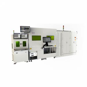
Using localized laser heating mechanism, temperature can be applied selectively in the interconnection areas of interest without heating up the entire substrate up to the reflow temperature to liquefy and reflow an interconnection of a few microns. With customized bond tool and laser technology, pick-and-place and assembly reflow heating are accomplished in single step at high accuracy <5µm. Localized heat ensures reliable bonding of large dies while the in-situ reflow supports ultra-small die assembly as small as 300µm.
Our unique temperature control mechanism protects single chip or component from being over-heated and prevents substrate from warpage and repeating reflow circumstances.
- Localized and selective heating with laser
- Flexible laser beam shaping
- In-situ reflow for low thermal stress
- Customizable bond tools
- High placement accuracy
- Suitable for bonding materials with CTE-mismatch

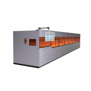
Our mask-less self-patterning wet chemical plating process applies Nickel, Palladium and Gold over the Aluminium or Copper bond pad on semiconductor wafers of different materials including Silicon, Silicon compound, Indium Phosphide, Lithium Tantalate etc. This layer acts as an adhesion layer, diffusion barrier, and wetting layer for the solders and wire bonds to enhance reliability and performance of various assembly and packaging such as Flip Chip and WLCSP. The wafers are loaded in a fully automated wet chemical plating line, where the wafers are handled by robot handler to go through chemical bathes which are well-controlled by in-line analysis and maintenance.
Talk to us to understand more about the unique turnkey model we offer for low to high volume production with either subcontracting services or equipment, chemical sales and technology transfer. We provide specific proprietary chemical compositions for a reproducible and reliable result, which has been proven with over 25 years of our in-house high volume manufacturing experience.
- Low cost high throughput
- Mask-less pad metallization
- Fully automated dry-in-dry-out wafer processing
- Capable of handling wafer size from 4” to 12” without tooling
- In-line bath analysis and maintenance
- Multi recipe management and SECS GEM interface available

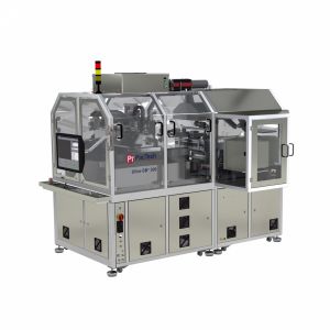
Ultra-SB2 is a fully automated solder bumping equipment integrating flux printing, ball placement, 2D inspection and wafer level rework prior to solder reflow to enable optimum bump yield on wafer up to 100%. The machine is capable of handling wafer from cassette to cassette, and the integrated 2D inspection is not only inspecting the wafer after ball placement, but also including pre- and post-placement stencil inspection to maximize solder bumping process control.
The solder balls are placed onto UBM pads of the pre-fluxed wafer and being fixed into position, enable high accuracy ball mounting especially for micro solder balls and fine pitch layouts. The wafer mounted with solder balls will be inspected again for missing, misplaced, extra solder balls and the rejects are removed and replaced prior to solder reflow. Ultra-SB2 is customizable to be integrated into existing manufacturing line via different wafer handling system to realize automatic wafer processing.
- Capable of handling 4″-12″ wafer
- Automated FOUP to FOUP robot handling
Optional integrated rework capability for optimum bump yield
- High accuracy
- Optional integrated flux printing and 2D AOI
- Customizable in-line manufacturing adaptation


